Schematic Entry and Board Layout
OrCAD Capture CIS
One of the most widely used and powerful schematic design solutions for the creation and documentation of electrical circuits. Take your product ideas from concept to production by utilizing the integrated part search dashboard, electrical rule checks, simulation support as well as hierarchical, reuse and variant design capabilities to improve productivity and get your designs right the first time.
Features:
- Hierarchical design: Organize schematics by specific functions for efficient design reuse, review, and editing.
- Unified search: Access up-to-date electronic parts and models directly within the design environment, eliminating the need for manual research.
- Design synchronization: Conduct real-time design rule checks and seamlessly transfer design data between schematic and PCB editor, ensuring consistent updates.
- Extensive model library: Gain access to a wide range of electronic parts and models, simplifying symbol placement and reducing the need for manual creation.
- Symbol editor: Easily create or modify schematic symbols within the environment, customizing pins and properties for precise design representation.
- Design difference viewer: Quickly identify and review differences between designs using side-by-side comparisons, enhancing efficiency and productivity.
PCB Designer
A tiered, scalable and powerful PCB design solution that delivers advanced capabilities and highly integrated flows that gives you the ability to expand as your designs and challenges increase in complexity. Take advantage of advanced place and route technology, 3D visualization, integrated signal integrity analysis, a constraint management system that provides real-time validation for length rules and more, as well as support for IPC-2581, STEP and IDX to streamline your manufacturing process.
Features:
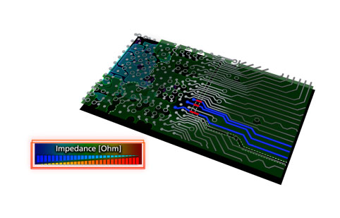
- Impedance Analysis: Visually identify impedance discontinuity issues without extensive signal integrity expertise or simulation models.
- Design Automation: Utilize auto-assisted design features, such as fanouts and via creation, to enhance productivity and save time when working with high pin-count devices like BGAs.
- Manufacturing: Easily create and assign manufacturing constraints based on IPC standards and common PCB rules to ensure design manufacturability.
- Miniaturization: Create and place blind, buried, and micro via stacks in high-density interconnect (HDI) and high-speed designs. Enable miniaturization and optimize space utilization.
- Design Reuse: Reuse proven design intellectual property (IP) to save time and effort by avoiding designing each project from scratch.
- 3D Rigid Flex: Visualize designs in interactive 3D to identify part collisions and ensure proper fit and functionality of the board, especially in rigid-flex designs.
- Design Rules: Manage PCB design rules using a simple spreadsheet-based interface. Capture design rules in a constraint-driven workflow and verify their compliance in real-time, reducing design time and stress during signoff.
- Shape Management: Define, edit, and dynamically update shapes without waiting for repouring polygons. Easily revise, reshape, and manage shapes during routing.
OrCAD PCB Productivity Toolbox
A comprehensive suite of utilities that improves the overall productivity and efficiency of PCB layout designers. Leverage a collection of design-time-reducing functions as well as advanced design-function enablers that enhance and optimize existing PCB layout capabilities.
Features:
- Polar Grid: Efficiently manage component placement and interconnect routing for circular boards.
- Label Tuning: Automatically optimize the location and rotation of component names on the silkscreen for improved manufacturability.
- Assign Net to Existing Via: Change the signal or net name on an existing via without deleting and re-adding it.
- Cross Copy: Copy elements to a different layer while preserving their original features.
- Barcode: Generate barcode images of design part numbers or custom information for tracking and identification.
- Batch Plot: Create a defined document batch for streamlined printing, such as generating PDFs.
- Padstack Finder: Locate and highlight padstacks in the design for easy identification and management.
- Post Processing: Generate manufacturing data in a specific order to meet manufacturers' requirements consistently.
OrCAD Free Viewer
A free download that lets you share and access a read-only version of your design data with your team for review and tracking progress of your design.
Features:
- License-free access: Open, view, and plot Allegro PCB Editor, OrCAD PCB Editor, Allegro Package Designer, and Allegro PCB SI technology databases without a license.
- Powerful search: Easily locate critical components, nets, vias, and measure their distances for optimized placement.
- Enhanced visibility controls: Adjust visibility settings to enhance the viewing experience and focus on specific elements.
- Documentation viewer: View manufacturing documentation generated by the Allegro PCB Manufacturing Option, OrCAD Documentation Editor, and OrCAD Panel Editor.
- Starter library: Access the Cadence Allegro/OrCAD Starter Library 1.0, which includes schematic symbols, PCB footprints, and component properties.
- Installation instructions: Follow provided instructions to install and utilize the Allegro/OrCAD Starter Library.
- Cross-Section Library Extension: Download and access an extended library of pre-solved cross sections for improved signal integrity analysis using Allegro SI products.
Design and Data Management
OrCAD Engineering Data Management
A comprehensive data management environment that helps you manage your design data in OrCAD Capture. Ensure data integrity and project status management while eliminating the challenges associated with managing files across multiple users, locations, and disciplines.
Features:
- Project dashboard: Provides a powerful dashboard for project visibility and team collaboration.
- Real-time traceability and communication: Tracks changes made by team members and offers real-time visibility into project status.
- Full version history: Maintains a complete version history for easy access and comparison of changes.
- Controlled release management: Freezes designs at a finished state to ensure integrity and manage updates.
- Project coordination: Centralized location to view, manage, and assign schematic pages and projects.
- Page locking: Automatically locks pages being edited to maintain data integrity.
- Library management: Enables editing and tracking of individual schematic symbols.
- Facilitates IP reuse: Stores and enables search for IP from previous designs.
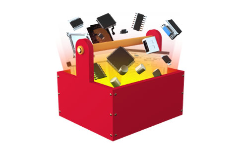
OrCAD Library Builder
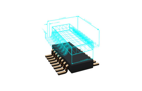
An automated solution for part creation. Advanced PDF datasheet extraction drives schematic symbol and PCB footprint/land pattern creation, eliminating traditional error-prone manual processes and creating accurate component libraries in a fraction of the time.
Features:
- Advanced and automated capabilities: OrCAD Library Builder provides advanced and highly automated features for quickly creating part symbols and footprints for OrCAD PCB schematics and layouts.
- Error elimination: The tool virtually eliminates errors caused by manual processes, improving design quality and reducing rework.
- Time-saving: OrCAD Library Builder reduces symbol and footprint creation processes from hours or days to just minutes, resulting in a dramatically accelerated workflow.
- PDF datasheet extraction: The solution utilizes advanced PDF data extraction technology to pull component data from any PDF datasheet, eliminating the need for manual content copying and pasting.
- Error checking and reporting utilities: OrCAD Library Builder automates error-prone tasks and provides a complete set of error-checking and reporting utilities, ensuring libraries are built correctly the first time and reducing costly rework.
- Template-based creation: The tool allows the creation of templates to ensure that all symbols and footprints adhere to common standards, promoting consistency and efficiency.
- Symbol creation: OrCAD Library Builder enables quick and accurate extraction of datasheet specifications, formatting, and data checking for symbol generation, streamlining the process and facilitating export to the schematic tool.
- Footprint creation: The solution provides a comprehensive set of land pattern calculators based on IPC-7351 specification, allowing input of dimensions directly from datasheets and ensuring industry-standard and consistent footprints.
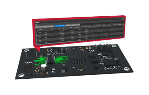
OrCAD Component Information Portal

A comprehensive database management and online component research environment that easily integrates into OrCAD Capture. The component information portal (CIP) enables design teams to quickly and cost-effectively realize the full benefits of a shared component database and effective component management process.
Features:
- Comprehensive Component Data Management: Manage component data effectively within OrCAD Capture CIS.
- Integrated Online Distributor Access: Access component parametric data from suppliers and vendors for efficient component research.
- Temporary Part Creation Process: Create temporary parts as placeholders in designs, streamlining the design process.
- User-Friendly Interface: Intuitive interface for adding, editing, and searching for parts.
- Streamlined Component Research: Integrated access to online distributors for millions of downloadable component content.
- CIS Database Setup and Management: Starter database of 5,000+ components, predefined schemas, and automated maintenance.
- User Roles and Data Access: Control access rights and ensure data integrity with user privileges and notifications.
- Web-Based Interface for Non-Users: Web-based access for non-OrCAD users, enabling collaboration with documentation, library development, and purchasing teams.
Simulation and Analysis
PSpice Designer
Leverage the industry-leading, native analog, mixed-signal, and analysis engines to deliver a complete circuit simulation and verification solution. Whether you�re prototyping simple circuits, designing complex systems, or validating component yield and reliability, you can rely on the best, high-performance circuit simulation and advanced analysis technology to analyze and refine your circuits, components, and parameters before committing to layout and fabrication.
Features:
- Advanced Circuit Simulation: PSpice delivers a complete circuit simulation and verification solution for analog and mixed-signal circuits.
- Circuit Optimization: Use PSpice's Advanced Analysis (AA) simulation engines to maximize design performance, yield, cost effectiveness, and reliability.
- Electro-Mechanical Simulation: Perform system-level simulation powered by PSpice and MATLAB Simulink for electro-mechanical system simulation.
- Transient Analysis: Analyze circuit response over time to understand the behavior of your design during state transitions.
- Smoke Analysis: Ensure component reliability by analyzing their behavior under changes in voltage, current, power, and temperature.
- Sensitivity Analysis: Identify critical components and parameters that have the most impact on circuit performance and evaluate yield versus cost tradeoffs.
- Monte Carlo Analysis: Predict circuit behavior under different conditions and calculate manufacturing yield using advanced statistical analysis.
- Optimizer: Fine-tune analog circuits to meet design requirements and performance goals by finding the best component or system values.
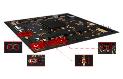
OrCAD PCB SI
An integrated analysis environment that delivers powerful simulation technology to help find and address signal integrity (SI) issues throughout the design process from circuit design in the schematic to board placement and routing. It enables pre- and post-layout topology exploration, signal analysis, and validation. Increase circuit reliability and drive known-good interconnect requirements throughout the PCB design flow to reduce re-spins.
Features:
- Pre- and post-layout capabilities for signal integrity exploration at any stage of the design cycle.
- Exploration, analysis, and design of interconnect topologies to improve circuit reliability and performance.
- Direct integration with OrCAD PCB Editor and OrCAD Capture for seamless workflow.
- Embedded constraints drive known-good interconnect requirements throughout the design flow.
- Support for industry-standard formats and models for flexibility and compatibility.
- Proven, scalable solution based on Cadence Allegro technology.
- Pre-layout analysis to proactively identify and address signal integrity issues early.
- Post-layout analysis validates layout against pre-route requirements and allows for modifications if needed.
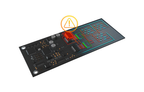
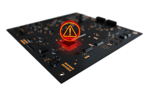
OrCAD Sigrity ERC
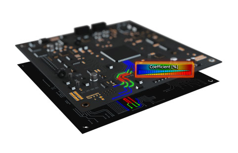
The Electrical Rules Check (ERC) enables PCB designers to screen a PCB design for signal quality without having to assign any simulation models or to be a signal integrity expert. Going beyond simple geometry-based DRC, the entire PCB design can be evaluated for impedance discontinuities, excessive crosstalk, and return path discontinuities. Reduce overall design time by not over-burdening the SI experts with signal quality issues that can be found and addressed during the PCB layout stage.
Features:
- Electrical rules checking without simulation models or expertise.
- Advanced signal quality analysis surpassing geometry-based DRC.
- Seamless integration with OrCAD PCB Editor for issue visualization and correction.
- Reduced design time with early identification and resolution of signal quality issues.
- Reference-aware analysis covering trace references, impedance, coupling, routing phase, and vias.
- User-friendly interface designed for PCB layout designers.
- Visual overlays for impedance and coupling identification.
- Comprehensive results tables for actionable insights and issue resolution.
Design for Manufacturing
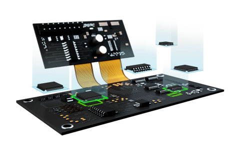
OrCAD Documentation Editor
A PCB documentation-authoring tool that intelligently automates your documentation creation process to produce complex PCB documentation in a fraction of the time versus traditional methods. Developed in the style and use-model of Windows desktop applications, you can quickly create the manufacturing drawings that drive PCB fabrication and assembly.
Features:
- Automated PCB documentation creation process.
- Intelligent linked PCB views, drawing details, and document notes.
- Efficient creation of fabrication, assembly, and inspection instructions.
- Drag-and-drop drawing elements for easy customization.
- Seamless integration with OrCAD PCB Editor for streamlined data transfer.
- Time-saving automation for generating component assembly views, drill patterns, and parts lists.
- Real-time updates of drawing elements with design changes.
- Support for advanced capabilities like geometric dimensioning and tolerance (GD&T) and blind/buried vias.
OrCAD Panel Editor
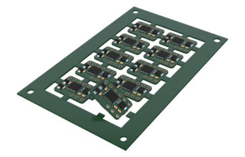
A PCB assembly ("array") panel design tool that intelligently automates the panel definition and documentation process to produce simple or complex PCB assembly panels in a fraction of the time versus traditional manual methods. Developed with a highly intuitive style and use-model, you can quickly design your panel and create the manufacturing drawings that drive fabrication and assembly.
Features:
- Automated panel definition and documentation process.
- Creation of simple or complex PCB assembly panels.
- Automatic array creation for optimized panel layouts.
- Quick placement of top, bottom, drill pattern, or custom panel arrays.
- Generation of drill charts, note blocks, mill and V-score details.
- Panel-level drill and coordinate charts for component placement and pick-and-place machinery.
- Automatic NC milling definition for route paths and break out tabs.
- Ease-of-use with drag-and-drop drawing elements and customizable formatting.
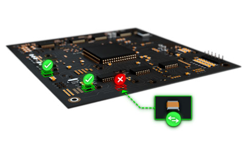
OrCAD DFM Checker
A comprehensive, easy to use PCB manufacturing analysis technology that identifies specific design issues that may have an adverse effect on PCB fabrication. Designs that pass standard design rule verification may unknowingly contain critical issues that could result in low manufacturing or assembly yields, or costly scrap. DFM Checker enables you to correct potential manufacturing issues before the design is sent to the fabricator to avoid time-to-market delays.
Features:
- Comprehensive analysis to identify design issues that can result in manufacturing and assembly problems.
- Hierarchical rule-set-driven analysis for easy management and customization of DFM checks.
- Creation and storage of checking routines for reuse on other designs, reducing duplication effort.
- PCB fabrication analysis to detect content that may affect fabrication, such as spacing, annular rings, and mask slivers.
- PCB assembly analysis to detect content that may affect assembly, including solder and paste mask features.
- Error charting for large-scale analysis, allowing for quick identification and resolution of failures.
- Tight integration with OrCAD PCB Editor for efficient error correction in the source PCB design.
- Cross-probing functionality to easily locate and correct errors within the PCB design.
