Annexure A PCB Design, Manufacturing, Assembly Development Plan and Process flow
Design Process flow:
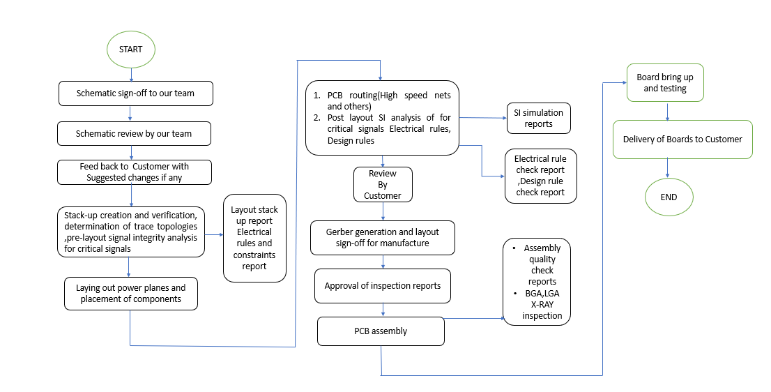
The following diagram enlists important milestones for completion of activities under Scope of work from the date of release of schematic sign-off:
Schematic Review:
We must conduct a review of schematics signed-off by Customer and seek clarifications if required. Also, we recommended the modifications/improvements to Customer if any. The BoM will be checked for obsolescence or near End of Life of components. We identify critical signal nets, such as clock signals or high-speed data lines, and ensure they are routed with care. we will Review differential pairs to ensure proper routing and length matching for consistent signal propagation.
Library creation:
All the footprints will be created as per the IPC 7351 standards and manufacturer’s datasheet recommended land patterns. Customer can provide the appropriate guidelines for landing patterns if any. Once done with the footprint creation your team will review the footprints with respective datasheets and organizational guidelines. We are Expertise in building and organizing PCB libraries using industry-standard. Capable of structuring libraries for efficient component management, version control, and compatibility with CAD software.
-
Pre-layout Signal Integrity analysis and validation
- We will identify the routing constraint requirements for high-speed sections/signals of the design. Pre-layout SI validation will be carried out to assess the layout requirements, stack-up build and to develop appropriate design rules and constraints.
- We will do the PCB laminate with RoHS compliance, suitable for High-speed signals like DDR3, Flash memory interface, Ethernet Interface (SGMII & RGMII), PCI Express Interface, stack up creation and trace topologies to meet controlled impedance requirements shall be determined in co-ordination with the PCB manufacturer and your hardware design team.
- Layout design constraints will be created based on the arrived pre-layout SI validation results.
PCB layout design
PCB layout design and generation of Gerber data shall be done by our engineers, using the schematic data signed-off by customer. The design rules and constraints developed by pre- layout analysis shall be applied to the layout database and applied to the design of the layout. We have Extensive experience in designing multilayer PCBs with a focus on optimizing signal integrity, power distribution, and thermal management. Skilled in routing high-speed and high-density designs while adhering to best practices for manufacturability and assembly.
-
PCB layout design will include the following tasks:
- Creation of board outline as per the dimensions got from customer.
- Placement of components to adhere the design constraints in particular cases and assessing routability of various components with considering ‘Design for Manufacture’ and ‘Design for Assembly guidelines. These guidelines give directions on recommended spacing between certain components, route/package/via keep-out areas. Recommended spacing clearance around BGA, LGA components to facilitate inspection, attachment of heat sinks shall be followed.
- We follow the datasheet recommended layout guideline for major component placement and routing with respect to the IPC 2221.
- Completion of routing of traces, adhering to design rules and constraints established in the pre- layout analysis of the board.
- Perform Design rule and database checks.
- We will perform the Signal Integrity (SI) Analysis for all high-speed signals like DDR3, Flash memory interface, Ethernet Interface (SGMII & RGMII), PCI Express Interface and other critical signals once done with the layout.
- Generate of Gerber files in RS 274-X type and will perform the QC.
Post-layout Signal Integrity simulation and validation of High-speed signals:
Before layout sign-off, post layout SI simulation and validation shall be carried out by your hardware team. The S-Parameter model extraction from the layout is done using the Electromagnetic 3D extraction for vias and other plated through holes, and 2D extraction for traces. A part from SI analysis we will do the basic PI(power integrity) Analysis as well.
Thermal analysis:
Thermal analysis shall be done to evaluate critical areas (E.g., at FPGA, Voltage regulator modules) for temperature rise and assess cooling requirements including air-flow and heat sink specifications. We use the industrial leading analysis tools to model the thermal behavior of PCBs, vias, and components to predict temperature profiles and identify potential hotspots.
PCB manufacture:
PCB manufacturing may be outsourced to the allied partner, using the Gerber files. RoHS manufacturing processes shall be followed. The manufactured PCB will meet the requirements of the standard IPC 6012, Class 2.PCB manufacturing notes and guidelines shall be provided to the manufacturer. PCB will be made with quality of FR4 grade Class-2, PCB thickness of 100 mil (or less) copper clad with glass epoxy lamination will be used. In the PCB Solder mask & legend will be print should be provided as per the industry standard process.
-
We will provide the below listed data/files to the manufacturer for PCB fabrication:
- Gerber Files: These are the standard files used by PCB manufacturers to generate the necessary production data. Include all layers of the PCB (top copper, bottom copper, solder mask, silkscreen, etc.) in RS274-X Format.
- Fab Drawings/Notes: Provide fabrication drawings or documentation specifying board dimensions, tolerances, materials, layer stack-up, and any special requirements for fabrication.
- Drill Files: Provide Excellon drill files (.drl) specifying the coordinates and sizes of all holes and vias in the PCB along with drill chart provided in the design.
- Special Instructions: Include any special instructions, notes, or requirements relevant to the manufacturing process, such as material specifications, surface finish preferences, or panelization requirements
PCB Assembly:
PCB assembling will be outsourced to our allied partner, using the Bill of Material provided by CUSTOMER along with PCB schematics. We will Procure all the components as per BOM. All components procured will be RoHS compliant and relevant conformity certificates to be obtained from the component manufacturers. Assembly quality check reports and BGA, LGA X-Ray inspection reports shall be submitted to customer if any. Acceptance of assembly will comply to IPC-A-610, Class 2.
Pick-and-Place (PnP) File:
This file provides assembly machine data, including component coordinates and rotation angles.
Assembly Drawings:
Include assembly drawings or documentation detailing component placement, orientation, and any special instructions for assembly.
Board Test and bring up:
PCB testing is a crucial step in the manufacturing process to ensure that assembled boards meet quality standards and perform reliably. Here are some common methods and strategies we use for testing PCBs:
Visual inspection of assembled boards:
By visual inspecting the overall appearance of the assembled board, checking for any obvious defects such as solder bridges, missing components, or physical damage. Proceed to inspect individual components, starting with critical components such as ICs, connectors, and fine-pitch components. Verifying component polarity and orientation, ensuring that all components are placed correctly according to the assembly drawings and component markings.
In-Circuit Testing (ICT):
ICT involves testing the electrical integrity of individual components and connections on the PCB using specialized test equipment. CT verifies component values, checks for opens, shorts, and incorrect placements, and ensures that the PCB functions within specified parameters. CT is especially useful for complex PCBs with densely populated components.
Power On - Functional Testing:
Functional testing evaluates the overall functionality of the assembled PCB by subjecting it to simulated operating conditions. This testing method verifies that the PCB performs its intended functions correctly, such as powering up, communicating with external devices, and processing inputs and outputs.
JTAG Test for Processor
Scan chain Test & hello world program, Flash Memory Read/Write though JTAG
JTAG (Joint Test Action Group) testing for processors, also known as boundary scan testing, is a method used to verify the functionality and connectivity of integrated circuits, including processors, on a printed circuit board (PCB).JTAG enables testing, debugging, and programming of devices on a PCB through a serial interface.
DDR3 memory test:
Testing DDR3 memory modules is crucial to ensure their reliability, performance, and compatibility with the target system. We will Prepare a test bench with the necessary hardware and software tools for memory testing.
FPGA interface test:
Testing the interface between an FPGA (Field-Programmable Gate Array) and other components or peripherals is essential to ensure proper communication, data transfer, and functionality.
000Base-X SFP (SGMII Interface) test:
Testing a 1000Base-X SFP (Small Form-factor Pluggable) module with an SGMII (Serial Gigabit Media Independent Interface) interface involves verifying its functionality, performance, and compatibility with the network infrastructure.
